In an effort to be more transparent about our development process and current project status, we will be trying something different moving forward. We will be sharing updates here as they happen and summaries will go on our blog.
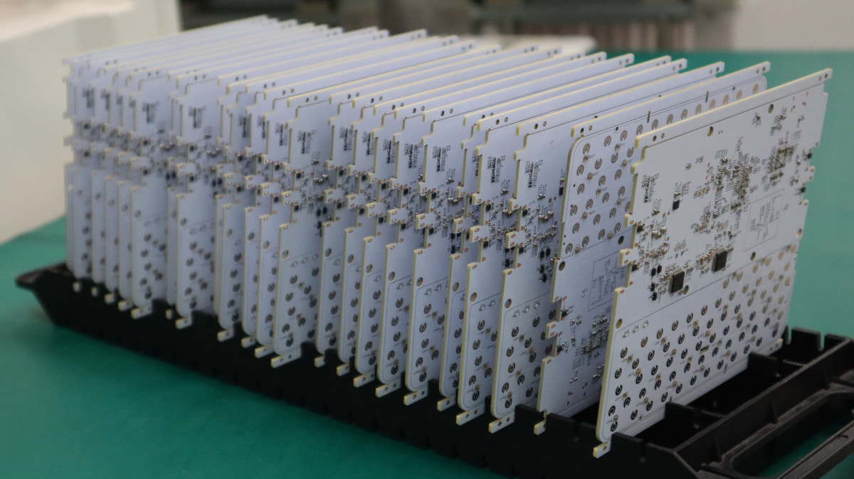
Since we are very close to having a complete D.V.T. 2 PCB ready for fabrication, we thought this would be a good point to share the work that goes into Design For Manufacturing (DFM) or “the final lap” so to speak of PCB development.
We have setup a GitHub repository for Pocket P.C. where the PCB design files once validated and completed for mass production will be posted.
The repository can be found here:
In this repository have posted a “Stackup” which is a high-resolution PDF file that includes all (10!) of the PCB layers and assembly drawings.
The PDF can be found here:
https://github.com/PopcornComputer/PocketPC-Hardware/tree/master/Stackup
Click on the PDF filename and it will take you to a page where you can click “Download”.
Here’s a preview of the bottom and top layer.
Note: The keyboard side is considered the bottom layer and the SoC / component side is considered the top layer.


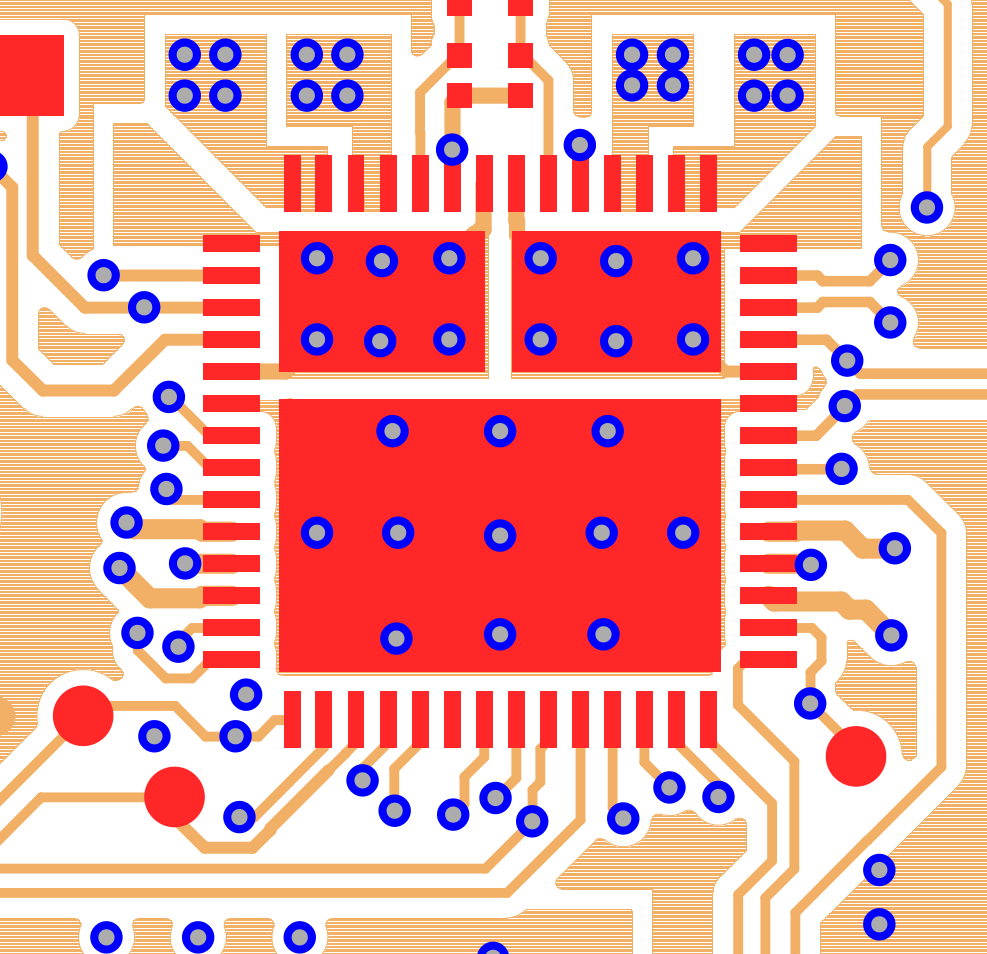
We are taking a multi-day review of the final stackup before sending the files out for production. We are marking areas of concern for our PCB design engineer to modify or review.
Here’s an example of a change request markup that we did on a previous revision.

In this photo we marked that “fins” should be added to the USB Power Delivery IC. These fins help dissipate heat from underneath the IC. The datasheet for this IC demonstrates these fins should be added in their recommended layout seen below.

After our engineer has made the change you can see the result below:
This is one of many minor changes we have been making the past few days. We expect to send the latest design out for production on Monday, July 27th.
In a previous revision, we created a 2 Layer PCB without any drills or traces and left only the footprints for the components. This allowed us to get a PCB back from the fabrication house within a few days. We used this special 2 Layer PCB to test the positioning of the connectors against the 3D prints.


With this PCB in hand, we hand soldered the connectors and fit it into the case.


And the result was almost perfect. Because we had checked multiple times the 3D PCB file against the mechanical design in CAD all the connectors where in the proper position. USB-C cables, SD card and battery fit perfectly. The only change we had to make was to clip the corners of the PCB so that it could be removed more easily.
That’s all for now. We welcome any questions about our process or the design. Let us know what you think below.